Time to read: 7 min
As data and connectivity continue to be popular themes in tech, engineers are increasingly tasked with packing more features into smaller products, which often leads to deeply integrated electromechanical designs and complex assemblies. This guide aims to outline a framework for electrical and mechanical engineers to identify easily overlooked PCB design issues, minimize revision cycles, and help keep all of those sweet features in your new product.
PCB Design: Where Mechanical & Electrical Engineering Intersect
As you probably already know, communication is critical when developing products with a team of individuals with specialized backgrounds. Communicating your needs to the team early and clearly gives you the best chance to catch conflicting design requirements and address them while designs are still in the CAD or schematic phase, resulting in a solution that’s cheaper, easier, and less painful to design.
The Prerequisites
Assuming your team has clear and reasonable product requirements, individuals can draw up initial mechanical and electrical designs. Envelope constraints and industrial design will drive mechanical design. Ergonomics, industry regulations, and limits of material properties will all be factors. Features outlined in the product requirements will drive electrical design.
Once the mechanical engineer (ME) has a working mechanical design, and the electrical engineer (EE) has a functional schematic, the team can start to design the printed circuit board (PCB).
PCB Outline & Keepouts
The first step in the process is agreeing on an initial PCB outline, which allows the design team to agree upon a size and shape for the PCB early on. The ME should provide a drawing that has the following key elements:
- Board Outline
- Areas with Height Restrictions
- Keepouts for Parts
- Keepouts for Traces
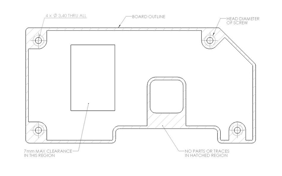
Board outline is obvious—this is the final shape of the PCB once it’s fabricated and largely depends on the mechanical design. Often, the ME can start by providing a drawing with the maximum PCB size possible, given the intended location in the mechanical design. If the schematic design permits, the ME can work with the EE to reduce the PCB outline to the smallest possible area, which will help reduce material cost.
Something to consider: Rectangular board outlines will result in cheaper cost compared to organic “curved” outlines, due to less wasted PCB material and more machine time required to route out the organic shape. When communicating the board outline, a maximum height constraint for electrical components should be included. In many cases, the maximum allowable height will not be the same at every place on the PCB due to mechanical constraints.
The outline drawing should note regions of the PCB that have height restrictions smaller than the maximum in order to avoid interference issues during assembly. “Keepouts for Parts” are areas where the mechanical enclosure touches the PCB or comes so close that there’s not enough clearance for small components. These areas should be communicated in a similar way as those with height restrictions.
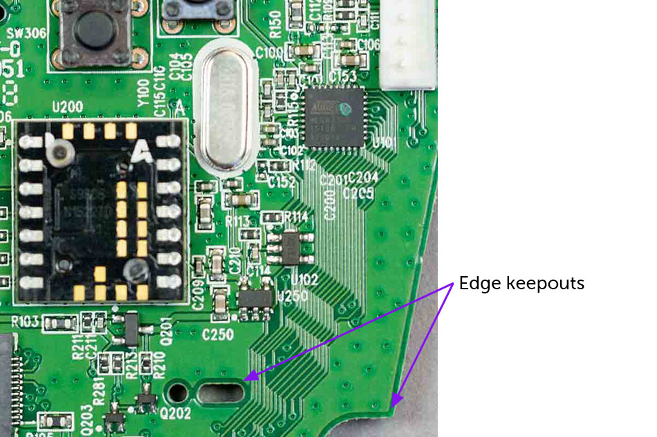
Finally, “Keepouts for Traces” are areas of the PCB that can’t have any traces. This can apply to a specific layer or all layers. For MEs, the main areas of concern early in the design cycle are regions where metal parts are located close to the PCB, mounting features, and edges of the board, including any internal cutouts.
There should always be a minimum distance from the edge of the board that can’t have any traces. The distance is dependent on the Voltage, Current, and Dielectric material of the PCB and is aimed at preventing electrical arcing.
If your product requires certification from a registered Safety Body, they will have minimum guidelines specific to your application. Otherwise, the latest IPC-9592B document is a good place to start. Note: If you’re using metal hardware to secure the PCB, include extra keepout space to take into account the diameter of the screw head.
It’s a common mistake to just offset from the through hole diameter, which can result in interference or shorting.
Layout
At this point, the EE can begin laying out the traces that connect the electrical components on the PCB. It’s best to start grouping all components into regions that have no height restrictions and slowing moving individual components or entire circuits composed of small components into regions with restrictions. The ME and EE should get together and identify a list of large, rare, or high-risk components.
Extra care should be taken when laying out these parts; spec sheets should be reviewed by all members of the team; and parts should be mocked up in CAD to make sure they integrate into the mechanical design without issue. The EE should identify areas of the PCB that have special requirements: AC vs. DC circuits, capacitive sensing, antennas, etc. Often, these special layout areas restrict placement of components.
When the layout is complete, most professional software packages will let you export the PCB in a 3D file format, which can be really helpful when components are tightly packaged. The ME should load the 3D file into the mechanical assembly for review. If everyone on the team signs off, and everything fits onto one PCB, congratulations! It’s your lucky day.
Complex Solutions: How to fit too many things into not enough space
At the end of the day, PCB layout is all about surface area. You only have so much area in which to place components, and as devices become more complex through connectivity, you often won’t have enough space to fit everything onto one PCB. Luckily, there are plenty of options to help you design around this problem.
Below are the pros and cons of some common solutions.
Add Layers To the PCB
In this case, there’s enough physical space to fit all of the components onto the board, but once the EE starts to route the traces and account for the required spacing to prevent electrical arcing, you can’t fit everything into the limited surface. Your best option is to add layers to the PCB, which will add some cost to your board. It’s fairly common for a PCB to have 1-8 layers, but they can have more if your design requires it.
Note: adding layers will increase the thickness or your PCB and could affect your overall assembly.
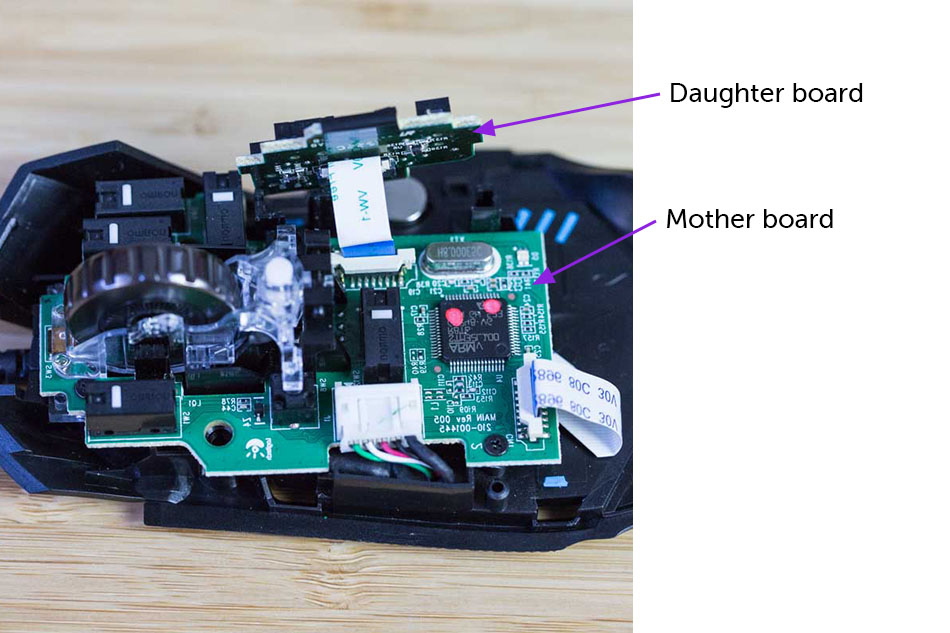
Daughter Boards
When you run out of space on your main PCB, the motherboard, usually the best and most cost-effective option is to move an entire circuit to a completely new PCB, the daughter board. Ideally, you want to move entire circuits over to a daughter board to reduce the number of required connections back to the motherboard. This will add some additional cost to your assembly, due to the added PCB, and will add complexity, because you need to find a way to mount the daughter board in your mechanical assembly and connect it to the motherboard.
This is still often the best option, because it’s easy to design a PCB with reliable mounting features and reliable off-the-shelf solutions to connect your boards together.
Note: this is also a good option if your design requires a sensor, button, or switch to placed in a location that is far away from the main PCB.
Move Large Components off the PCB
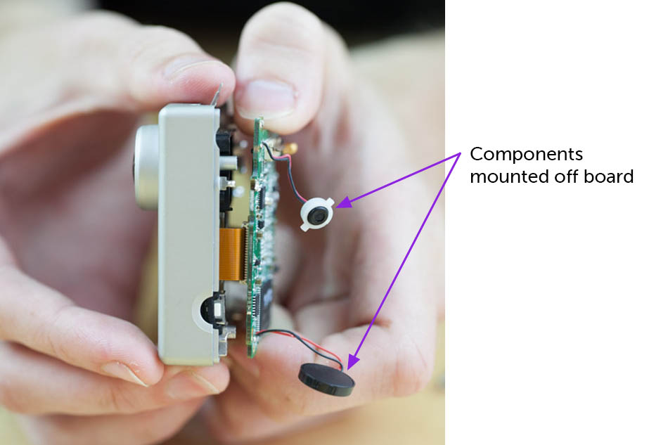
In certain situations, you may only have one or two large components—maybe a filtering capacitor, inductor, or third party sensor module, that prevent you from designing a small compact PCB and sliding it into a nice small corner of your mechanical package. Don’t be afraid to get creative and move one or two of these components somewhere else in the package if it frees up your design.
If your package will be injection molded, you can design custom mounting features to hold these components directly into your package. Then, connect them back to the PCB with flying leads.
Connecting Everything Together
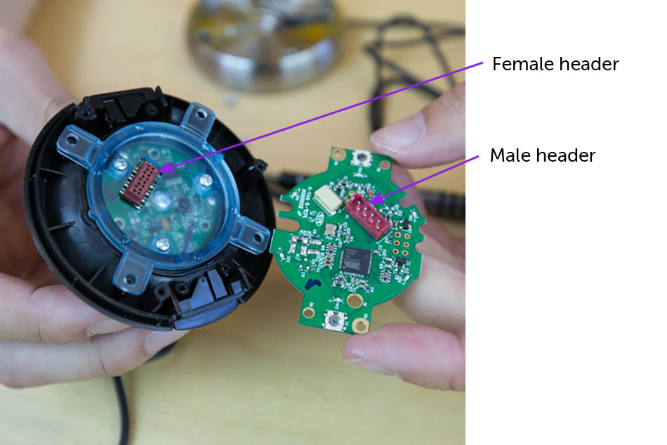
Now that we’ve split our circuits up between a mother board and one or more daughter boards, we need to connect everything back together in a way that’s both cost-effective and reliable. If you require a lot of circuit connections between your two PCBs, and you have the space, a horizontal or vertical header is likely your best option. It’s a common solution, with many off-the-shelf options. The downside is that headers themselves typically take up a lot of surface area on the PCB.
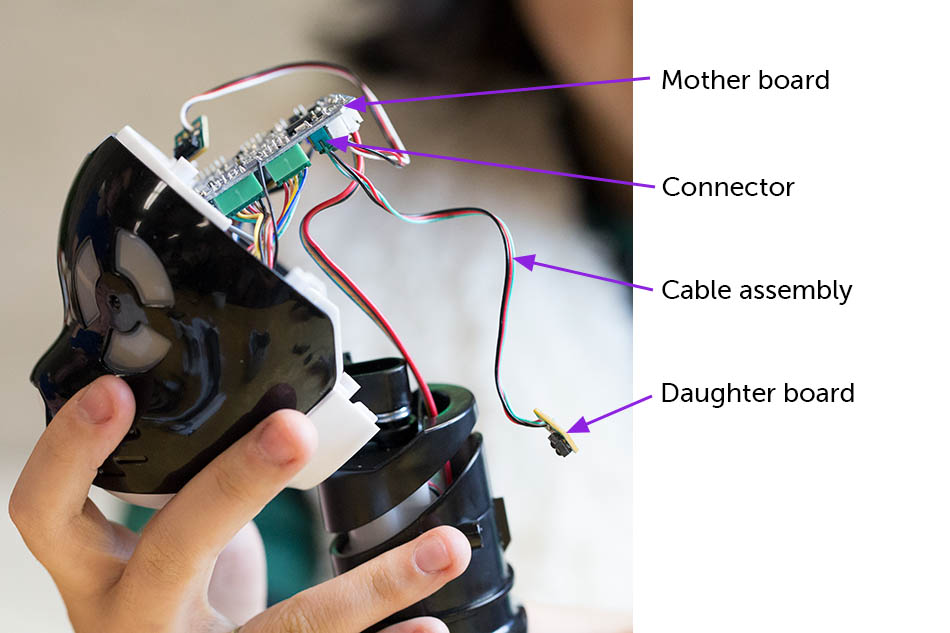
If a header doesn’t work in your design, the next best option might be a custom cable assembly. Again, these are common and provide a more flexible solution than headers, because the cable assembly can be tailored to your needs.
Cables can be any length you need. Connectors can be placed anywhere on either PCB and don’t necessarily need to match up like headers. This will add slightly more cost than headers because of the labor required to make the cable assembly. Keep in mind the order of operations of product assembly!
It’s possible to design a solution in CAD space that can’t be reasonably assembled, which can cause major redesign pain if you get too far along before you catch it. Another thing to note: Headers and cable assembly connectors are larger for higher power connections, due to minimum spacing to prevent electrical arcing. Large connectors often won’t work in tightly packaged assemblies, which is why it’s always best to move low power circuits to daughter boards.
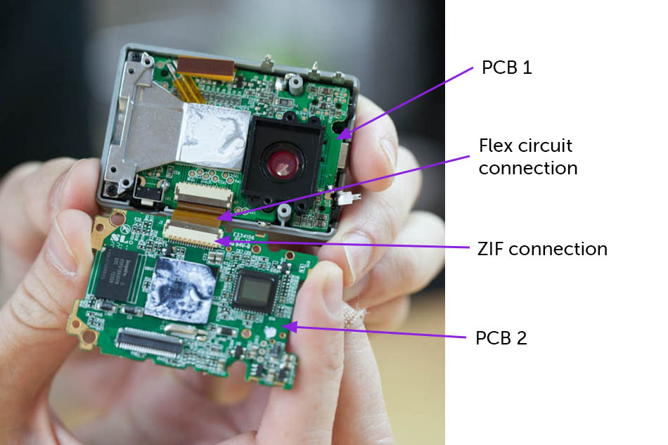
When space constraints outweigh cost constraints, your best option is probably a flex connector or circuit, which are essentially printed circuit boards, but instead of using fiberglass as the substrate, the circuits are printed on flexible kapton. This lets you bend and fold the connector as needed, with the benefit of only being 0.1-0.2 mm thick for a single layer circuit.
Like cable assemblies, flex circuits are custom-tailored to your design and can be cost-effective in high volumes, but they can get expensive in lower volumes, due to the tooling required to cut out the shape of the flex circuit. Flex connections can be soldered directly to the PCB, or use ZIF connectors.
Main Takeaways
Many factors go into PCB design that require input from multiple stakeholders. Being able to identify and de-risk spatial constraints early in the product development lifecycle will minimize the number of iterations it takes to get it right. Cost and reliability should always be chief concerns when everything doesn’t fit nicely onto one PCB, as is often the case. Hopefully, this playbook gives you the inspiration you need to get creative with your PCB design.

